The goal of next-generation HBM5 memory specification is to double performance and increase power efficiency compared to HBM4E, Samsung announced at the 'Memory Executive Summit,' an event that precedes 'Semicon Taiwan 2026.' Considering that it is barely realistic to double the data transfer rate of HBM4E in just one generation, the comment made by Samsung may imply that HBM5 will double the number of interface pins to boost bandwidth.
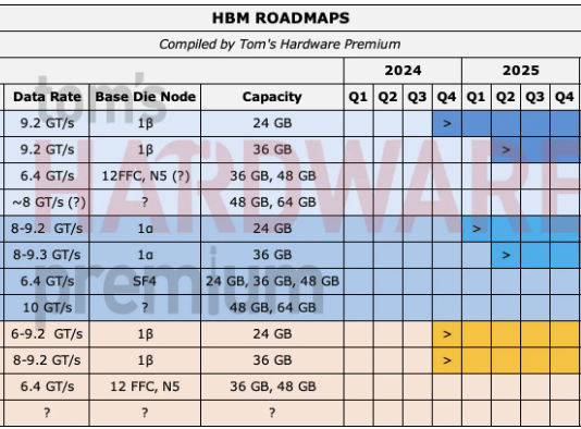
The goal of HBM5, which is currently under development, is to double the performance and improve the performance per watt by 20% compared to the HBM4E generation, according to Choi Jang-seok, the head of the product planning team of the memory business department of Samsung Electronics DS division. Previously, Samsung announced that its HBM5 memory stacks will feature a heat path block (HPB), which will reduce thermal resistance by 20% and simplify cooling of HBM5 modules.
Doubling HBM5’s per-stack memory bandwidth would result in peak bandwidth of around 4 TB/s per stack already in 2028 – 2029. TSMC expects AI accelerators to get to 20 – 24 HBM5/HBM5E per package configurations by the end of the decade, which means that these systems-in-packages will get a whopping 80 TB/s – 96 TB of memory bandwidth just several years down the road.
Although both DRAM makers like Micron, Samsung, or SK hynix as well as developers of HBM controllers and PHYs like Cadence, Rambus, or Synopsys already offer HBM4/HBM4E controllers and interfaces rated for 16 GT/s data transfer rates, the official JEDEC transfer rate for HBM4E will be around 12 GT/s.
If Samsung expects HBM5 to deliver twice the bandwidth of HBM4E, the HBM5 specification must either double the per-pin data transfer rate from 12 GT/s to 24 GT/s, double the interface width from 2,048 to 4,096 bits, or combine a wider interface with a higher data transfer rate. Increasing HBM5 memory stack interface width to 4,096 bits has so far been envisioned by KAIST and Marvell; however, this is certainly not an even semi-official confirmation of the specification's target.
From a performance-per-watt perspective*, widening the interface is generally easier than doubling the per-pin signaling rate. Higher per-pin speeds require faster drivers, receivers, clocks, equalization, tighter timing margins, and a more sophisticated PHY since maintaining signaling integrity at speeds well beyond 20 GT/s is not easy. But while a wider HBM interface moves more bits in parallel at a lower speed per wire, going from 2,048 to 4,096 pins means twice as many TSV/I/O paths, drivers, receivers, bumps, more complicated routing, and extremely complicated base die. So while a 4,096 I/O at moderate speed is probably best for pJ/bit, the interface/package complexity gets so extreme that it may offset the gains. Furthermore, such a wide interface Perhaps a 3,072-bit interface combined with a moderate increase in data transfer rate would be a reasonable engineering compromise, though engineers involved in JEDEC’s decision-making process may think otherwise. In any case, for now, any discussion of HBM5 specifications remains speculative.
Nonetheless, the target to double the bandwidth of HBM4E (2 TB/s per stack) within one generation is clearly a very aggressive one.
*It should be noted that achieving a 20% higher energy efficiency can be achieved not only by increasing performance, but by improving DRAM process technology, optimizing base die, lowering TSV I/O voltages, architectural changes, or power management.