微信内可能无法直接打开本站。请点右上角 ··· → 在浏览器打开,或复制链接。
Extending 18A With Significant Power And Performance Gains
RSS 官方收录 · 可信分层展示
关键摘要
With Intel 18A, Intel Foundry introduced industry-first technologies with RibbonFET Gate-all-around (GAA) transistor architecture and PowerVia backside power delivery in a production-ready process designed for high-volume manufacturing.…
- Intel 18A-P, the first performance-enhanced node in the Intel 18A fami…
- ² In research presented at the 2026 IEEE/JSAP Symposium on VLSI Techno…
- At the top end of the portfolio, RibbonFET with Power Boost technology…
摘要引擎:抽取
正文提要
With Intel 18A, Intel Foundry introduced industry-first technologies with RibbonFET Gate-all-around (GAA) transistor architecture and PowerVia backside power delivery in a production-ready process designed for high-volume manufacturing. Intel 18A-P, the first performance-enhanced node in the Intel 18A family, builds on that foundation to deliver more than 9% higher performance at the same power or over 18% lower power at the same performance compared to Intel 18A.²
In research presented at the 2026 IEEE/JSAP Symposium on VLSI Technology and Circuits, our team of Intel Foundry technologists achieved these gains through a combination of new RibbonFET device options, transistor and interconnect enhancements, and design-technology co-optimization (DTCO). At the top end of the portfolio, RibbonFET with Power Boost technology and enhanced strain engineering delivers additional performance optimization for applications such as AI accelerators, mobile devices, and data centers. Strain engineering improves transistor speed performance by carefully tuning mechanical stress in the channel region, allowing charge carriers to move more efficiently and increase drive current. This dual contact device option boosts drive current through ultra-low-resistance contacts, enabling higher frequencies at matched capacitance.

Intel 18A-P maintains the same SRAM cell design offerings and matched SRAM minimum operating voltage as Intel 18A while remaining fully design-rule compatible with Intel 18A. This allows customers to leverage existing design flows, IP, libraries, and infrastructure while benefiting from the technology’s performance and efficiency improvements, further reducing migration effort and accelerating time-to-market.
Breaking the performance-power tradeoff
AI and other modern computing workloads continue to drive demand for greater performance and energy efficiency. However, increasing performance has traditionally required more power, creating challenges for cooling, operating costs, and system scalability. Intel took a major step toward breaking this tradeoff with Intel 18A. RibbonFET provides tighter control of transistor switching behavior, while PowerVia moves power routing to the backside of the wafer, reducing wiring congestion and improving efficiency. Continuing this innovation, new transistor architectures, lower-resistance interconnects, improved thermal characteristics, and DTCO refinements enable Intel 18A-P to achieve meaningful gains in both frequency and power efficiency for a broad range of workloads.
A novel approach: Enhancing the technology foundation
Intel 18A-P expands the RibbonFET portfolio with new device options optimized for different design goals (see Figure 1). These options significantly enhance the technology offering for both power efficient designs as well as high-performance compute designs. New low-power W1 and W1.5 devices offer lower capacitance, reducing the energy required to switch transistors on and off, providing additional flexibility for power-sensitive designs. At the high-performance end of the portfolio, Intel 18A-P introduces W3P devices featuring Power Boost. These high-performance contacts allow transistors to operate more than 10% faster without increasing the electrical load associated with switching, helping improve performance while preserving power efficiency.²
Enabled by PowerVia backside power delivery, Power Boost’s dual contact architecture improves transistor performance through ultra-low-resistance contacts (see top image above). By providing both a conventional frontside contact and a direct backside contact, the architecture reduces resistance and increases drive current without increasing transistor footprint or capacitance.
Compared to Intel 18A, the new architecture lowers external resistance by approximately 20% for NMOS devices and 12% for PMOS devices, enabling higher drive current and higher operating frequencies at matched capacitance.² As a result, Power Boost helps designers extract more performance from the same silicon area, improving efficiency in power-constrained and performance-sensitive designs.
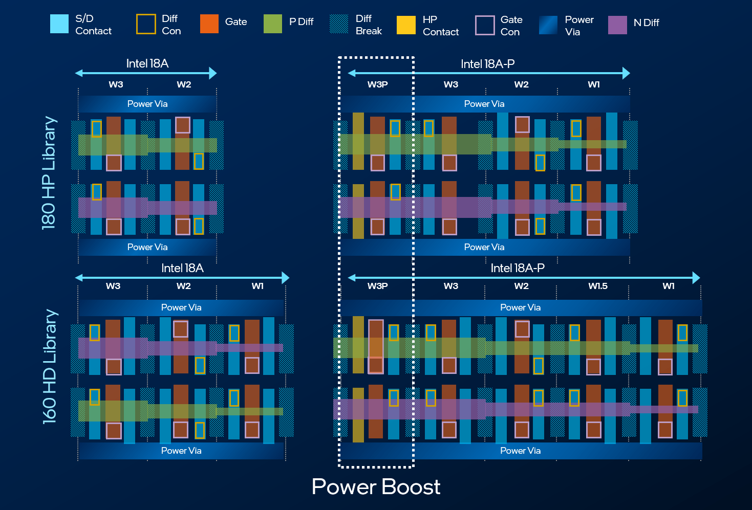
Fig. 1: Intel 18A-P offers new low-power W1 and W1.5 devices and high-performance W3P devices with Power Boost.
Intel 18A-P also gives designers greater flexibility through additional threshold-voltage (VT) options. The process technology adds an intermediate logic VT pair between existing low-voltage and ultra-low-voltage offerings, providing more granular control over the tradeoff between performance and power consumption. Combined with approximately 33% tighter skew corners, these enhancements make transistor behavior more predictable across manufacturing conditions, allowing designers to tune performance and power more precisely while reducing the need for conservative design margins.²
Key findings: Measurable gains across the board
These technology enhancements translate into measurable improvements at both the device and block levels. On an industry-standard ARM core sub-block, Intel 18A-P delivered over 9% faster performance at the same power level compared to Intel 18A — or viewed the other way, more than 18% lower power use at the same speed (see Figure 2).²

Fig. 2: Intel 18A-P achieves higher speed at the same power draw compared to Intel 18A on a standard processor core test block.
These gains resulted from the combined impact of all technology enhancement elements, including greater design flexibility, expanded device options, and intrinsic improvements in transistor switching speed. On Intel 18A-P, circuit-level switching speed is approximately 12% faster, driven by higher transistor drive currents in both NMOS and PMOS devices. Intel 18A-P delivers approximately 5% higher NMOS drive current and 16% higher PMOS drive current compared to Intel 18A. Both enhancements are enabled by the Power Boost architecture’s ultra-low-resistance contacts, while additional PMOS gains result from enhanced strain engineering. Interconnect enhancements further contribute to overall circuit level frequency gains. Via resistance is reduced by 10% to 30% in performance-critical routing layers, while metal jogs improve signal efficiency throughout the design. Together, these enhancements help customers achieve higher performance without increasing power budgets.²
Importantly, all performance gains were achieved while matching or improving reliability compared to Intel 18A. Intel 18A-P improves PMOS long-term reliability by reducing negative bias temperature instability (NBTI) degradation while maintaining strong gate oxide and hot-carrier reliability. These reliability metrics, which assess the ability of transistor materials and insulating layers to withstand years of operating stress, remain aligned with Intel 18A targets.
Improved thermal management for sustained performance
As computing workloads become increasingly demanding, thermal management plays an equally important role in overall system performance. AI training, inference, high-performance computing (HPC), and modern data center applications often operate at high utilization for extended periods, making efficient heat removal essential to sustaining peak performance.
Building on the thermal innovations introduced with Intel 18A, Intel 18A-P further improves heat dissipation through material enhancements and advanced EDA-driven thermal solutions. Intel 18A-P improves the bond stack thermal conductance by 50%, leading to an overall 20-40% improvement in the thermal resistance of the overall stack.²·³ The result is a process technology better equipped to support the performance and power densities required by next-generation AI, HPC, and cloud workloads, helping customers sustain peak performance under demanding operating conditions.
Built for manufacturing efficiency
Advanced chip technologies such as backside power delivery can increase manufacturing complexity, so Intel 18A-P was designed to balance innovation with cost efficiency. The technology shares the same interconnect stack as Intel 18A and uses extreme ultraviolet (EUV) lithography to pattern lower metal layers, helping reduce frontside process complexity. These advantages help offset the cost of backside processing and provide customers with a practical path to higher performance and improved energy efficiency without taking on the cost and complexity of a new design platform.
A foundation for future innovations
Intel 18A-P represents the first performance-enhanced node in the Intel 18A family, demonstrating our approach to continuous technology evolution. Looking ahead, Intel Foundry plans to continue expanding the Intel 18A platform with future derivatives and next-generation process technologies, including Intel 18A-PT and Intel 14A.
As AI, cloud, edge, and client computing continue to demand greater performance within fixed power budgets, Intel 18A-P provides customers with a practical path to deliver more capability, greater efficiency, and faster time-to-market while preserving existing Intel 18A design investments in next-generation products.
Endnotes
- Anupama Bowonder led the Intel 18A and Intel 18A-P transistor development team for Intel Foundry. See the full list of contributors.
- “Intel 18A-P CMOS Technology Enhancement Featuring Advanced RibbonFET (GAA) Transistors and PowerVia for High-Performance Computing,” IEEE/JSAP Symposium on VLSI Technology and Circuits, June 2026.
- “Backside Power: Enabling Energy-Efficient Performance on Advanced Node Designs,” IEEE/JSAP Symposium on VLSI Technology and Circuits, June 2026.
The post Extending 18A With Significant Power And Performance Gains appeared first on Semiconductor Engineering.